
Kyocera to build two new plants for ceramic components supporting IoT and 5G
- Corporate
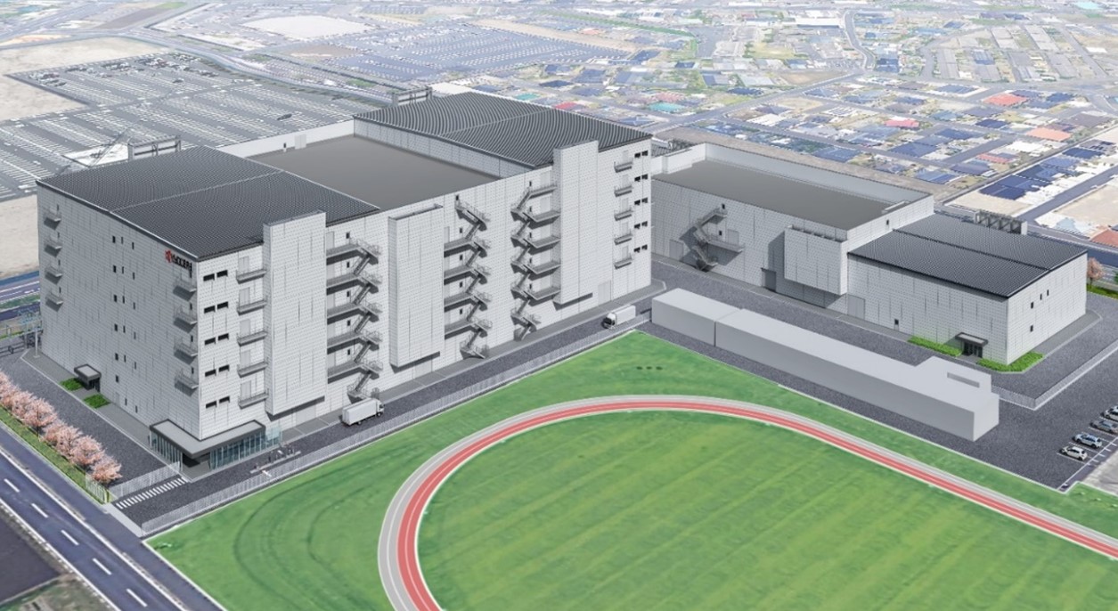
Kyoto/London − Kyocera announced that it will construct two additional production facilities at its Kokubu Plant Campus in Kagoshima, Japan, to serve customers worldwide. The new facilities will double the campus’ production capacity for fine ceramic components used in semiconductor manufacturing equipment, while securing space for other manufacturing as Kyocera’s business expands. A signing ceremony held on October 20, 2021 included Kagoshima Governor Koichi Shiota, Kirishima City Mayor Shinichi Nakashige, and Kyocera officials. Construction is scheduled to begin in November 2021.
Kyocera expects its fine ceramic business expansion to stimulate economic development in Kagoshima Prefecture and create new employment opportunities in the community.
Outline of New Facilities
| Name |
Plants No.7-1 & 7-2 at Kyocera’s Kagoshima Kokubu Plant Campus |
||
|---|---|---|---|
| Address | 1002-1 Kokubukamikogawa, Kirishima-shi, Kagoshima Prefecture, Japan | ||
| Total investment |
Approximately 11 billion yen (approx. 97 million U.S. dollars) | ||
| Building footprint |
No.7-1: 5,174 m2 (55,692 f2), steel construction, 2 stories No.7-2: 6,996 m2 (75,304 f2), steel construction, 6 stories |
||
| Total area |
No.7-1: 10,120 m2 (108,931 f2) / No.7-2: 37,497 m2 (403,614 f2) |
||
| Construction plan |
No.7-1: Construction to begin November 2021 Facility to open October 2022 No.7-2: Construction to begin November 2021 Facility to open October 2023 |
||
| Production items |
Fine ceramic components for semiconductor manufacturing equipment used in IoT, 5G telecommunications and other applications |
||
| Expected production level |
Approximately 3.4 billion yen (approx. 30 million U.S. dollars) per year (April 2023-March 2024) |